全部博文(200)
分类:
2013-01-07 14:29:11
原文地址:基于ARM的电源管理 作者:garyybl
1. 系统工作状态
几乎所有的ARM处理器设计都有空闲模式。在空闲模式状态下,处理器的时钟停止,以减少处理器在空闲状态下的功耗。当嵌入式操作系统发现处理器当前没有可执行的任务时,便将处理器置于空闲状态。当系统发生中断时,处理器从空闲状态被唤醒。大多数系统都有操作系统计时器中断,因此,处理器在一秒钟之内可能几千次的进出空闲状态。
值得注意的是,处理器空闲模式仅影响处理器本身,对系统的其他硬件不产生任何影响。系统的各状态切换如图所示。
图1显示了基本的电源管理和工作状态。
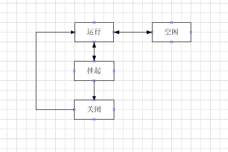
图1系统的状态切换
2. 系统挂起模式
在系统挂起模式(也称睡眠模式)下,只有以下部件继续工作:SDRAM、处理器功耗管理电路、唤醒电路。
因为SDRAM里面的内容受到保护,系统的运行状态可以存入SDRAM里保存。以下是进入睡眠模式的典型步骤。
(1)用户指定、超时、低电量状态等因素启动了挂起模式。
(2)操作系统调用驱动程序把外设调整到节电状态。
(3)处理器未保存的寄存器存入SDRAM。
(4)SDRAM进入自刷新模式。
(5)处理器进入挂起模式。在该模式下,处理器的时钟停止,系统中各供电模块关闭。
重新恢复的次序与挂起次序相反,由处理器的唤醒信号或处理器内部唤醒信号源(如实时计时警报)启动。系统执行挂起模式是个庞大的任务,必须了解如何将系统中所有的外设切换到节电状态。
3.系统关闭状态
对ARM系统来说,挂起状态虽然已大大减小了功耗,但系统在挂起状态下也消耗能量,因而需要一种关闭模式,像系统没有电源一样。这种模式在电池耗尽时可以有效地保护电池不被损坏;同时可使系统在安装有电池的情况下进行传输和储存。
4.软启动
大多数系统需要一种软启动功能,软启动时,处理器被复位,但是SDRAM里面的内容仍旧保持。目前,大部分便携式系统都选择在SDRAM中存储用户文件,这是一项非常有用的功能。
---------------------------------------------------------------------------------------------------------------------===================---------
以下翻译自S3C2440A手册:
POWER MANAGEMENT
The Power Management block controls the system clocks by software for the reduction of power consumption in the S3C2440A. These schemes are related to PLL, clock control logics (FCLK, HCLK, and PCLK) and wakeup signals.Figure 7-7 shows the clock distribution of the S3C2440A.
The S3C2440A has four power modes. The following section describes each power management mode. The transition between the modes is not allowed freely. Please see Figure 7-8 for available transitions among the modes.
电源管理
在S3C2440A中,电源管理模块通过用软件管理的方式控制系统时钟达到减少电源的消耗的目标。这些调度和PLL,时钟控制逻辑(FCLK,HCLK和PCLK)和唤醒信号相关。图7-7显示了S3C2440A的时序分布图。S3C2440A有4种电源模式。下面介绍每种电源模式。各个模式之间是不允许自由的转换。这些模式中可以进行如图7-8所示的模式转换。
NORMAL Mode
In Normal mode, all peripherals and the basic blocks including power management block, the CPU core, the bus controller, the memory controller, the interrupt controller, DMA, and the external master may operate completely. But, the clock to each peripheral, except the basic blocks, can be stopped selectively by software to reduce the power consumption.
IDLE Mode
In IDLE mode, the clock to the CPU core is stopped except the bus controller, the memory controller, the interrupt controller, and the power management block. To exit the IDLE mode, EINT[23:0], or RTC alarm interrupt, or the other interrupts should be activated. (EINT is not available until GPIO block is turned on).
正常模式:
在正常模式下,所有的外围设备和基本的模块包括电源管理模块,CPU内核,总线控制器,内存控制器,中断控制器,DMA,和外部控制器等。但是,除了基本必需的模块,对于每个外围设备可以通过软件管理的方式进行有选择的停止时钟用以减少电量的消耗。
空闲模式:
在空闲模式下,时钟对于CPU内核来说是停止的,但是对于总线控制器,内存控制器,中断控制器和电源管理模块来说,时钟是仍然处于工作状态。当外部中断EINT[23:0],RTC 告警中断或者其他中断被激活的时候,系统会退出空闲模式。需要注意的是,外部中断EINT在GPIO模块被打开之前是不能被使用的。
SLOW Mode (Non-PLL Mode)
Power consumption can be reduced in the SLOW mode by applying a slow clock and excluding the power consumption from the PLL. The FCLK is the frequency of divide_by_n of the input clock (XTIpll or EXTCLK) without PLL. The divider ratio is determined by SLOW_VAL in the CLKSLOW control register and CLKDIVN control register.
In SLOW mode, PLL will be turned off to reduce the PLL power consumption. When the PLL is turned off in the SLOW mode and the user changes power mode from SLOW mode to NORMAL mode, then the PLL needs clock stabilization time (PLL lock time). This PLL stabilization time is automatically inserted by the internal logic with lock time count register. The PLL stability time will take 300us after the PLL is turned on. During PLL lock time, the FCLK becomes SLOW clock.
Users can change the frequency by enabling SLOW mode bit in CLKSLOW register in PLL on state. The SLOW clock is generated during the SLOW mode. Figure 7-11(Please check the figure correctly) shows the timing diagram.
慢速模式(非锁相环模式)
在慢速模式下,电源的消耗可以通过应用一个慢速时钟,同时在PLL中排除电源的消耗。FCLK在没有PLL的状态下是输入时钟信号(XTIpll 或者 EXTCLK)的n分频,分频率是由CLKSLOW和CLKDIVN控制寄存器中的SLOW_VAL值来决定的。
在慢速模式下,为了减少PLL的电源消耗PLL将会被关闭。当PLL在慢速模式下被关闭,用户可以改变电源工作模式从慢速模式到正常模式,此时,PLL需要时钟稳定时间(PLL锁定时间)。这个PLL稳定时间被内部逻辑用锁定时间统计寄存器自动地插入。在PLL锁定时间和FCLK变成慢速时钟的这段时间内,PLL稳定的时间在PLL打开后大约消耗300us。
在锁相环状态,用户可以改变频率通过使能CLKSLOW 寄存器中的SLOW mode位。慢速时钟是在慢速模式下产生的。
SLEEP Mode
The block disconnects the internal power. So, there occurs no power consumption due to CPU and the internal logic except the wake-up logic in this mode. Activating the SLEEP mode requires two independent power sources. One of the two power sources supplies the power for the wake-up logic. The other one supplies other internal logics including CPU, and should be controlled for power on/off. In the SLEEP mode, the second power supply source for the CPU and internal logics will be turned off. The wakeup from SLEEP mode can be issued by the EINT[15:0] or by RTC alarm interrupt.
Follow the Procedure to Enter SLEEP mode
1. Set the GPIO configuration adequate for SLEEP mode.
2. Mask all interrupts in the INTMSK register.
3. Configure the wake-up sources properly including RTC alarm. (The bit of EINTMASK corresponding to the wake-up source has not to be masked in order to let the corresponding bit of SRCPND or EINTPEND set. Although a wake-up source is issued and the corresponding bit of EINTMASK is masked, the wake-up will occur and the corresponding bit of SRCPND or EINTPEND will not be set.)
4. Set USB pads as suspend mode. (MISCCR[13:12]=11b)
5. Save some meaning values into GSTATUS[4:3] register. These register are preserved during SLEEP mode.
6. Configure MISCCR [1:0] for the pull-up resisters on the data bus, D[31:0]. If there is an external BUS holder, such as 74LVCH162245, turn off the pull-up resistors. If not, turn on the pull-up resistors. Additionally, The Memory concerning pins is set to two types, one is Hi-z, and the other is Inactive state.
7. Stop LCD by clearing LCDCON1.ENVID bit.
8. Read rREFRESH and rCLKCON registers in order to fill the TLB.
9. Let SDRAM enter the self-refresh mode by setting the REFRESH[22]=1b.
10. Wait until SDRAM self-refresh is effective.
11. Set MISCCR[19:17]=111b to make SDRAM signals(SCLK0,SCLK1 and SCKE) protected during SLEEP mode
12. Set the SLEEP mode bit in the CLKCON register.
睡眠模式
电源模块断开内部电源,因此,在这种模式下,由于CPU和内部模式逻辑,此时是没有电源消耗的。激活休眠模式需要两个独立的电源供应源。其中一个电源供应源为唤醒逻辑提供电源,另一个电源供应源提供了其他的内部逻辑包括CPU,并且为了电源的开/关是可以被控制的。在睡眠模式下,为CPU和内部逻辑提供电源的第二个电源供应源将会被关闭。通过外部中断[15:0]或者RTC告警中断可以将系统从睡眠模式中唤醒。图7-9描述了进入睡眠模式的过程。
1. 设置GPIO寄存器为休眠模式
2. 在内部中断源屏蔽寄存器中屏蔽所有的内部中断
3. 适当地配置唤醒源,使其包括RTC告警
4. 设置USB为挂起模式
5. 将当前一些需要保留的值存储在寄存器GSTATUS[4:3]中,这些寄存器在睡眠模式下将被保留。
6. 在数据总线上将寄存器MISCCR [1:0]配置为上拉电阻
7. 清LCD控制寄存器1 LCDCON1的ENVID位来停止LCD的工作
8. 读取rREFRESH和rCLKCON寄存器中的值来填充页表缓存
9. 通过设置REFRESH[22]为1bit,让SDRAM进入自刷新模式
10. 等待,直到SDRAM自刷新模式开始运转
11. 设置MISCCR[19:17]为111bit,使得SDRAM的信号(SCLK0,SCLK1 and SCKE)在睡眠模式下得到保护
12. 设置CLKCON寄存器的睡眠模式比特位
Follow the Procedure to Wake-up from SLEEP mode
1. The internal reset signal will be asserted if one of the wake-up sources is issued. It’s exactly same with the case of the assertion of the external nRESET pin. This reset duration is determined by the internal 16-bit counter logic and the reset assertion time is calculated as tRST = (65535 / XTAL_frequency).
2. Check GSTATUS2[2] in order to know whether or not the power-up is caused by the wake-up from SLEEP mode.
3. Release the SDRAM signal protection by setting MISCCR[19:17]=000b.
4. Configure the SDRAM memory controller.
5. Wait until the SDRAM self-refresh is released. Mostly SDRAM needs the refresh cycle of all SDRAM row.
6. The information in GSTATUS[3:4] can be used for user’s own purpose because the value in GSTATUS[3:4] has been preserved during SLEEP mode.
7. – For EINT[3:0], check the SRCPND register.
– For EINT[15:4], check the EINTPEND instead of SRCPND (SRCPND will not be set although some bits of EINTPEND are set.).
Power Control of VDDi and VDDiarm
In SLEEP mode, VDDi, VDDiarm, VDDMPLL and VDDUPLL will be turned off, which is controlled by PWREN pin. If PWREN signal is activated(H), VDDi and VDDiarm are supplied by an external voltage regulator. If PWREN pin is inactive (L), the VDDi and VDDiarm are turned off.
图7-10描述了从睡眠模式唤醒的过程。
1. 如果发出一个唤醒源,内部重置信号将会被置位
2. 检查GSTATUS2[2]的状态,检查电源上电是否从睡眠模式下唤醒导致的
3. 通过设置MISCCR[19:17]为000bit来释放SDRAM保护信号
4. 配置SDRAM内存控制器
5. 等待SDRAM自刷新模式被释放。
6. GSTATUS[3:4]中的信息可以被用户使用,因为GSTATUS[3:4]的值在睡眠模式下已经被保护
7. 对于外部中断EINT[3:0], 检查待处理中断源寄存器SRCPND.对于外部中断EINT[15:4], 检查待处理外部寄存器EINTPEND
VDDi和VDDiarm的电源控制
在睡眠模式下,VDDi, VDDiarm, VDDMPLL和VDDUPLL将会被关闭,它们是由PWREN引脚控制。如果PWREN引脚处于高电平,VDDi和VDDiarm由外部电压调节器提供电源。如果PWREN引脚处于低电平,VDDi和VDDiarm则处于关闭状态。
http://www.cnblogs.com/Torres_fans/archive/2010/07/29/1788214.html
